
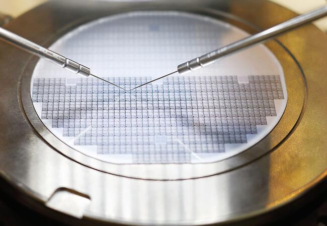
In the fast-paced world of semiconductor manufacturing, silicon wafers play a crucial role. These thin, circular slices of pure silicon serve as the foundation for manufacturing integrated circuits (ICs) and other electronic components. However, the production of these wafers is an intricate and resource-intensive process. Consequently, any unused or discarded wafers can result in a significant loss for manufacturers. This is where Wafer Reclaiming comes into the picture.
What is Wafer Reclaiming?
Wafer reclaiming, also known as wafer recycling or wafer reclaim, is a process that aims to recover value from discarded silicon wafers. Instead of sending these wafers to landfills, where they would be wasted, wafer and reclaiming involves refurbishing them to remove any contaminants or defects and restoring them to a usable state. This reclaimed wafer can then be reintroduced into the manufacturing process, thereby reducing waste and saving costs.
Benefits of Wafer Reclaiming:
· Cost Reduction
One of the primary benefits of wafer reclaiming is the significant cost reduction it offers to semiconductor manufacturers. Producing silicon wafers is an expensive endeavor, involving multiple stages of fabrication and stringent quality control measures. By reclaiming discarded wafers, manufacturers can avoid the high costs associated with producing new wafers from scratch. This cost-saving opportunity can be particularly advantageous for companies operating in a highly competitive market.
· Environmental Sustainability
In addition to cost savings, wafer, and reclaiming aligns with the principles of environmental sustainability. The semiconductor industry is known for its high resource consumption and waste generation. By reclaiming and reusing wafers, manufacturers can reduce their environmental footprint by minimizing the need for raw materials and decreasing the amount of waste sent to landfills. This practice contributes to a more sustainable and eco-friendly approach to semiconductor manufacturing.
· Enhanced Supply Chain Efficiency
Another advantage of wafer reclaiming is the improved efficiency it brings to the semiconductor supply chain. By reusing wafers, manufacturers can mitigate the risks associated with wafer shortages or supply chain disruptions. In situations where the availability of new wafers is limited or lead times are extended, wafer in reclaiming offers a viable alternative to maintain production without interruptions. This increased flexibility enhances the overall resilience and efficiency of the supply chain.
The Process of Wafer and Reclaiming:
· Wafer Collection and Sorting
The first step in the wafer reclaiming process is the collection of discarded wafers. These wafers can come from various sources, including the manufacturing floor, test facilities, or even customer returns. Once collected, the wafers undergo a thorough sorting process to separate those that are suitable for reclaiming from those that are not. This sorting process typically involves visual inspection, automated measurements, and sometimes non-destructive testing techniques to identify wafers with salvageable value.
· Cleaning and Removal of Contaminants
After sorting, the selected wafers move on to the cleaning stage. During this step, the wafers are subjected to a series of cleaning processes to remove any contaminant residues that may have accumulated on the wafer surfaces. Various cleaning techniques, such as chemical etching, ultrasonic cleaning, and plasma cleaning, may be employed to achieve the desired level of cleanliness. Once cleaned, the wafers are ready for the next phase of the reclaiming process.
· Surface Planarization and Reconditioning
In the surface planarization and reconditioning stage, any defects or imperfections on the wafer surfaces are addressed. This step is crucial to restore the wafers to their optimal condition for reuse. Surface planarization techniques, such as chemical-mechanical polishing (CMP) or grinding, are employed to remove any surface irregularities, scratches, or damaged areas. This process helps to ensure that the wafer surfaces are flat, smooth, and free from any defects that could negatively impact subsequent manufacturing processes.
· Thin Film Removal and Etching
In certain cases, wafers may have thin films or layers deposited on their surfaces, such as metal or oxide films, that need to be removed before they can be reclaimed. Thin film removal techniques, including wet etching, dry etching, or plasma stripping, are utilized to selectively remove these layers without damaging the underlying silicon substrate. This step is crucial to ensure the wafers' compatibility with the specific requirements of subsequent device fabrication processes.
· Quality Testing and Verification
Once the cleaning, surface planarization, and thin film removal processes are completed, the reclaimed wafers undergo a series of rigorous quality testing and verification procedures. These tests aim to assess the wafers' electrical and structural integrity, ensuring that they meet the required specifications for reuse. Various inspection techniques, such as optical microscopy, scanning electron microscopy (SEM), and electrical testing, are employed to evaluate the wafers' quality and identify any remaining defects or performance deviations.
· Wafer Reintegration into Manufacturing
After successfully passing the quality testing phase, the reclaimed wafers are ready to be reintegrated into the semiconductor manufacturing process. They can be used for various purposes, including the fabrication of new ICs, test structures, or as substrates for research and development activities. Reclaimed wafers are typically tracked and identified separately from new wafers to ensure proper documentation and control throughout the manufacturing flow.
Challenges and Considerations:
While wafer reclaiming offers significant benefits, there are several challenges and considerations that manufacturers must address:
· Contamination Control
Maintaining strict contamination control measures throughout the wafer and reclaiming process is essential to prevent the reintroduction of defects or contaminants. Any residue impurities can adversely impact the performance and reliability of the reclaimed wafers. Implementing robust cleanroom protocols and quality control procedures is vital to minimize the risk of contamination during wafers and reclaiming.
· Yield and Performance Variability
Reclaimed wafers may exhibit yield and performance variability compared to new wafers. The presence of residual defects or deviations from the original wafer specifications can impact the overall yield and performance of the manufactured devices. Manufacturers must carefully evaluate the trade-offs between cost savings and potential yield losses when incorporating reclaimed wafers into their production processes.
· Compatibility with Advanced Technologies
As semiconductor technologies continue to advance, the compatibility of reclaimed wafers with advanced manufacturing processes becomes a consideration. Newer technologies, such as extreme ultraviolet (EUV) lithography or three-dimensional (3D) integration, have stringent requirements that may pose challenges for reclaimed wafers. Manufacturers need to assess the feasibility and limitations of using reclaimed wafers in these cutting-edge technologies.
· Intellectual Property and Security
Reclaimed wafers may contain valuable intellectual property (IP) or sensitive data that needs to be protected. Manufacturers must implement robust protocols to ensure the secure handling and disposal of any reclaimed wafers that may contain proprietary or confidential information. Proper data sanitization techniques, such as wafer destruction or data wiping, should be employed to safeguard against potential IP or security breaches.
Future Trends and Innovations:
The field of wafer reclaiming is continuously evolving, driven by advancements in materials science, process technologies, and industry demands. Some notable future trends and innovations in wafer, reclaiming include:
· Advanced Defect Detection and Repair Techniques
To improve the quality and reliability of reclaimed wafers, there is a growing focus on developing advanced defect detection and repair techniques. This involves the use of high-resolution imaging technologies, such as electron beam inspection (EBI) or atomic force microscopy (AFM), to detect and characterize even the smallest defects on the wafer surface. Additionally, innovative repair methods, such as laser annealing or localized etching, are being explored to address specific defects and enhance the reclaiming process.
· Nanotechnology and Nanowire Reclaiming
With the emergence of nanotechnology and the increasing use of nanoscale devices, there is a rising interest in the reclamation of nanowires and other nanoscale structures. Wafer Reclaiming techniques are being adapted to handle these delicate and intricate structures, allowing for the recovery and reuse of nanowires from discarded wafers. This development has the potential to unlock new opportunities for sustainable nanoscale device fabrication.
· Integration of Artificial Intelligence and Machine Learning
Artificial intelligence (AI) and machine learning (ML) are being integrated into wafer and reclaiming processes to enhance efficiency and accuracy. AI algorithms can assist in defect detection, classification, and automated decision-making, reducing human error and optimizing the selection of wafers for reclaiming. ML models trained on vast datasets can also help predict the performance and yield of reclaimed wafers, enabling manufacturers to make informed decisions on their integration into the manufacturing flow.
· Wafer Reclaiming for Emerging Technologies
As new technologies continue to emerge, such as the Internet of Things (IoT), wearable electronics, and renewable energy systems, there is a growing need for specialized wafer materials and substrates. Wafer and reclaiming processes are being adapted to cater to the requirements of these emerging technologies. This includes the reclamation of wafers with specific characteristics, such as flexible or transparent substrates, to support the development of novel devices and applications.
· Circular Economy Approaches
Wafer reclaiming aligns with the principles of a circular economy, where resources are reused, recycled, and regenerated. Manufacturers are increasingly adopting circular economy approaches to minimize waste generation and maximize the value extracted from discarded wafers. This involves establishing collaborations and partnerships throughout the semiconductor supply chain to promote the exchange and reclamation of wafers, fostering a sustainable ecosystem within the industry.
Conclusion:
Wafer reclaiming offers a multitude of benefits to semiconductor manufacturers, including cost reduction, environmental sustainability, and enhanced supply chain efficiency. By reclaiming discarded wafers and restoring them to a usable state, manufacturers can minimize waste, conserve resources, and optimize their production processes. Although challenges exist, advancements in defect detection, nanotechnology, AI integration, and circular economy approaches are paving the way for a more efficient and sustainable wafer and reclaiming industry.